Semiconductors Java Physics
Junzo TAKAHASHI Instiyute of High-Tecnology
これは、英語ページです。日本語ページにジャンプできます。


話題の ISDN
でインターネット高速接続!
Do you use my force!(looking for a job)
Fields of Semiconductors(GaAs, SOI)

-- brief personal record--
Domicile:Miyagi,Japan in
1947
Degree:Ph.D. from TOHOKU University
Job:Manager of R&D Div. in
Japan Energy Co.Ltd., Hitachi Co.Ltd.
----Example
of GaAs Device similation---- 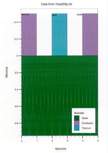
Structure of GaAs FET,
Gate length=1 μm,
Mesh points= 3000,
important part(channel)was meshed finely
----Presice Information----
1.List of Publication

DVD がすぐ届く!到着日が選べる!

ゲームソフト通信販売!
新作ソフトが発売日にお手元に届きます!
 ***
jtaka@super.email.ne.jp*2000/01/09***
***
jtaka@super.email.ne.jp*2000/01/09***