1-5.本研究の目的
本研究の目的は、様々の技術的課題を克服し、以上述べてきたような特長が期待される集束イオンビーム直接蒸着法を実現し、その特長を明らかにし、有用な新しい一つの微細加工手段、成膜手段として確立することである。
集束イオンビーム直接蒸着法を実現するための第一の技術的課題は、低エネルギーの集束イオンビームをいかに実現するかにある。イオンビーム蒸着に適当なイオンエネルギーは30~200eV程度である。一般的に低エネルギーのイオンビームは弱い電界に対しても敏感であること、空間電荷の影響を受けやすいことなどの理由により、その制御、輸送は容易でなく、低エネルギーイオンビーム用の光学系の設計は至難の業である。そのため、通常はある程度加速した状態でイオンビームを輸送し、使用する直前で必要なエネルギーまで減速する。集束イオンビームにおける低エネルギー化の試みは、直接蒸着をめざした先駆的な試み79)が報告されている。この報告ではエネルギーが150eVのCu、Geの混合イオンビームが10μm程度のビーム径で蒸着することが示されている。著者の研究はこの試みを引き継ぎ、1μm以下の微細なビーム径を持つ質量分離された低エネルギービームを用いて集束イオンビーム直接蒸着法を実用的な一つの新しい微細加工・成膜手法として確立したことである。そのほか、主にイオン注入時における誘起欠陥を低減する目的のために低エネルギーのGa+ビームの研究が1980年代の終わり頃よりおこなわれている80~82)。これらは目的も使用するイオン種も異なるが、低エネルギーの集束イオンビームを得ようと試みた点では同じである。特にPease等は、1μmにせまるビーム径を持つ50eVのGa+ビームを報告し、技術的に低エネルギー集束イオンビームが可能であることを示した。著者も、一度加速したイオンビームをターゲット基板直前の減速場により集束しつつ減速し必要な最終エネルギーを得る光学系と、利用するイオン種を単一化する質量分離器を合わせ持つ集束イオンビーム装置を設計製作し、低エネルギー集束イオンビームを得た。この過程は第2章において詳しく述べる。
また、直接蒸着用の液体金属イオン源の開発も著者がおこなった技術的課題である。これまでの液体金属イオン源は、Gaかイオン注入用に開発されたものしかなかったため、直接蒸着のための導電体用、超伝導体用、磁性体用のイオン源の開発をおこなった。この過程は第3章において述べる。
集束イオンビーム直接蒸着法自体が世の中に確立されていない新技術であるため、成膜した薄膜の評価方法、応用等についてもすべて模索しつつ進めていく必要があり、これらに関しても非常に大きな技術的課題であると言うことが出来る。これらに対する著者の試みは第4章、第5章において述べる。
1-6.本研究の内容
以上、本研究の主題である集束イオンビーム直接蒸着法に関し、母体となる二つの技術、すなわち集束イオンビーム技術とイオンビーム蒸着技術について回顧し、集束イオンビーム直接蒸着法に対して何を期待することが出来るかを議論してきた。
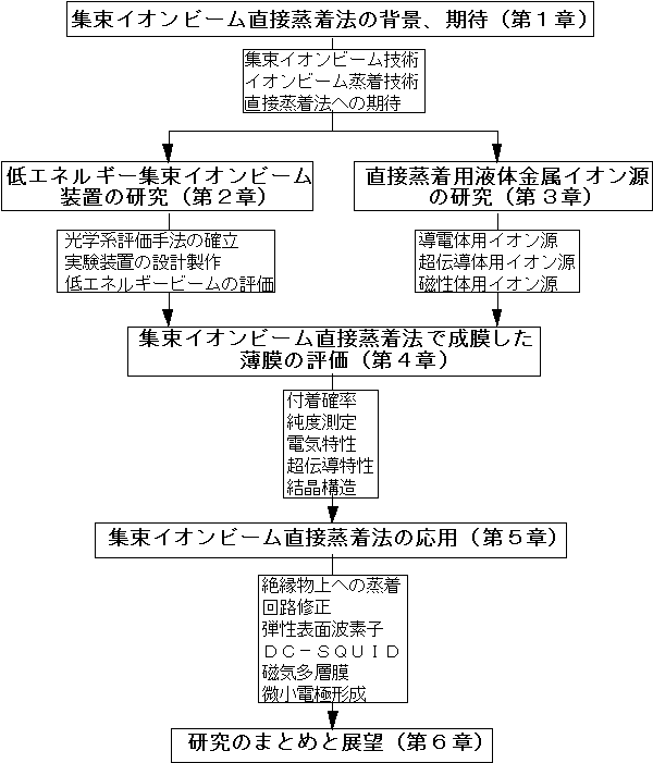
第2章においては、集束イオンビーム直接蒸着法を実現するために最も大きな技術的課題である低エネルギー集束イオンビームを開発した過程、すなわち光学系評価手法(シミュレーション手法)の確立、それを用いた低エネルギー集束イオンビーム装置の設計、同装置の製作、および得られた低エネルギー集束イオンビームの特性について述べる。
第3章においては、もう一つの技術的課題である直接蒸着に用いるための液体金属イオン源に関して、合金を用いた液体金属イオン源の特長、イオン源の構造(含浸電極型液体金属イオン源)、開発した導電体用液体金属イオン源、超伝導体用液体金属イオン源、および磁性体用液体金属イオン源について述べる。
第4章においては集束イオンビーム直接蒸着法で成膜した薄膜の評価について、付着確率の測定、蒸着膜の純度測定、蒸着膜の電気特性、蒸着膜の超伝導特性、および蒸着膜の結晶構造について述べる。
第5章においては、集束イオンビーム直接蒸着法の応用に関し、絶縁物上への蒸着、回路修正への応用、弾性表面波素子への応用、Nb系SQUIDへの応用、磁気多層膜への応用、および微小試料に対する電極形成について述べる。
最後に第6章において、本研究において得られた成果をまとめ、集束イオンビーム直接蒸着法が今後どのような基礎的な研究手段として利用できるか、またどのような実用的な応用技術として展開が可能であるかについて議論する。
本研究のフロー図を、図1-8に示す。
図1-8.本研究の内容フロー図
第1章の参考文献
1) G.Taylor : "Disintegration of water drops in an electric field", Proc. of the Royal Society A280 (1964) 383.
2) D.S.Swatik and C.D.Hendricks : "Production of Ions by Electrohydrodynamic Spraying Techniques", AIAA Journal 6 (1968) 1596.
3) V.E.Krohn : "Electrohydrodynamic capillary source of ions and charged droplets", J.Appl.Phys. 45 (1974) 1144.
4) V.E.Krohn and G.R.Ringo : "Ion source of high brightness using liquid metal", Appl.Phys.Lett. 27 (1975) 479.
5) R.L.Seliger, J.W.Ward, V.Wang and R.L.Kubena : "A high-intensity scanning ion probe with submicrometer spot size", Appl.Phys.Lett. 34 (1979) 310.
6) Kratos 社カタログ(LMIG50).
7) E.Miyauchi, T.Morita, A.Takamori, H.Arimoto, Y.Bamba and H.Hashimoto : "Maskless ion beam writing of precise doping patterns with Be and Si for molecular beam epitaxially grown multilayer GaAs", J.Vac.Sci.Technol. B4 (1986) 189.
8) J.S.Huh, M.I.Shepard and J.Melngailis : "Focused ion beam lithography", J.Vac.Sci.Technol. B9 (1991) 173.
9) S.Matsui, Y.Kojima and Y.Ochiai : "High-resolution focused ion beam lithography", Appl. Phys.Lett. 53 (1988) 868.
10) W.Chu, A.Yen, K.Ismail, M.I.Shepard, H.J.Lezec, C.R.Musil, J.Melngailis, Y.C.Ku, J.M.Carter and H.I.Smith : "Sub-100-nm X-ray mask technology using focused-ion-beam lithography", J.Vac.Sci.Technol. B7 (1989) 1583.
11) H.Morimoto, H.Onoda, T.Kato, Y.Sasaki, K.Saitoh and T.Kato : "Unique resist profiles with Be and Si focused ion beam lithography", J.Vac.Sci.Technol. B4 (1986) 205.
12) J.Melngailis : "Focused ion beam lithography", Nucl.Instrum.Methods B80/81 (1993) 1271.
13) W.M.Clark, R.L.Seliger, M.W.Utlaut, A.E.Bell, L.W.Swanson, G.A.Schwind and J. B.Jergenson : "Long-lifetime, reliable liquid metal ion sources for boron, arsenic and phosphorus", J.Vac.Sci.Technol. B5 (1987) 197.
14) E.Miyauchi, H.Hashimoto and T.Utsumi : "Au-Si-Be Liquid metal ion source for maskless ion implantation", Jpn.J.Appl.Phys. 22 (1983) L225.
15) R.H.Reuss, D.Morgan, A.Goldenetz, W.M.Clark, D.B.Rensch and M.Utlaut : "Fabrication of bipolar transistors by maskless ion implantation", J.Vac.sci.Technol. B4 (1986) 290.
16) S.D.Chu, J.C.Corelli, A.J.Steckl, R.H.Reuss, W.M.Clark, D.B.Rench and W.G.Morris : "Comparison of NPN transistors fabricated with broad beam and spatial profiling using focused beam ion implantation", J.Vac.Sci.Technol. B4 (1986) 375.
17) W.M.Clark, M.W.Utlaut, R.H.Reuss and D.Koury : "High-gain lateral pnp bipolar transistors made using focused ion beam implantation", J.Vac.sci.Technol. B6 (1988) 1006.
18) R.L.Kubena, J.Y.Lee, R.A.Jullens, R.G.Brault, P.L.Middleton and E.H.Stevens : "Si MOSFET fabrication using focused ion beams", IEEE Trans.Electron Devices 31 (1984) 1186.
19) J.Y.Lee and R.L.Kubena : "Threshold adjustments for complementary metal-oxide- semiconductor optimization using B and As focused ion beams", Appl.Phys.Lett. 48 (1986) 668.
20) H.Hamadeh, J.C.Corelli, A.J.Steckl and I.L.Berry : "Focused Ga+ beam direct implantation for Si device fabrication", J.Vac.Sci.Technol. B3 (1985) 91.
21) A.F.Evanson, J.R.A.Cleaver and H.Ahmed : "Focused ion implantation of gallium arsenide metal-semiconductor field effect transistors with laterally graded doping profiles", J.Vac. Sci.Technol. B6 (1988) 1832.
22) K.Nakamura, T.Nozaki, T.Shiokawa, K.Toyoda and S.Namba : "Fabrication of submicron isolation region in GaAs by Ga focused ion beam implantation", J.Vac.Sci.Technol. B5 (1987) 203.
23) E.Miyauchi and H.Hashimoto : "Application of focused ion beam technology to maskless ion implantation in a molecular beam epitaxy grown GaAs or AlGaAs epitaxial layer for three Dimentional dimentional pattern doping crystal grown", J.Vac.Sci.Technol. A4 (1986) 933.
24) T.Hiramoto, K.Hirakawa and T.Ikoma : "Fabrication of one-dimentional GaAs wires by focused ion beam implantation", J.Vac.Sci.Technol. B6 (1988) 1014.
25) Y.Hirayama and H.Okamoto : "GaAs/AlGaAs material modifications induced by focused Ga ion beam implantation", J.Vac.sci.Technol. B6 (1988) 1018.
26) P.M.Petroff, Y.J.Li, Z.Xu, W.Beinstingl, S.Sasa and K.Ensslin : "Nanostructures processing by focused ion beam implantation", J.Vac.sci.Technol. B9 (1991) 3074.
27) R.L.Seliger, R.L.Kubena,R.D.Olney, J.W.Ward and V.Wang : "High-resolution, ion-beam processes for microstructure fabrication", J.Vac.Sci.Technol. 16 (1979) 1610.
28) N.Matsunami, Y.Yamamura, Y.Itikawa, N.Itoh, Y.Kazumata, S.Miyanaga, K.Morita and R.Shimizu : "Energy dependence of sputtering yields of monatomic solids", IPP Nagoya Univ. Report IPPJ-AM-14 (1980).
29) H.Morimoto, Y.Sasaki, Y.Watanabe and T.Kato : "Characteristics of submicron patterns fabricated by gallium focused-ion-beam sputtering", J.Appl.Phys. 57 (1985) 159.
30) H.Yamaguchi, A.Shimase, S.Haraichi and T.Miyauchi : "Characteristics of silicon removal by fine focused gallium ion beam", J.Vac.Sci.Technol. B3 (1985) 71.
31) J.G.Pellerin, D.P.Griffis and P.E.Russell : "Focused ion beam machining of Si, GaAs, and InP", J.Vac.Sci.Technol. B8 (1990) 1945.
32) Y.Ochiai, K.Gamo and S.Namba : "Pressure and irradiation angle dependence of maskless ion beam assisted etching of GaAs and Si", J.Vac.Sci.Technol. B3 (1985) 67.
33) Y.Ochiai, K.Shihoyama, T.Shiokawa, K.Toyoda, A.Matsuyama, K.Gamo and S.Namba : "Characteristics of maskless ion beam assisted etching of silicon using focused ion beams", J.Vac.Sci.Technol. B4 (1986) 333.
34) M.Komuro and H.Hiroshima : "Focused Ga ion beam etching characteristics of GaAs with Cl2", J.Vac.Sci.Technol. B9 (1991) 2656.
35) L.R.Harriot, R.E.Scotti, K.D.Cummings and A.F.Ambrose : "Micromachining of integrated optical structures", Appl.Phys.Lett. 48 (1986) 1704.
36) T.Ishitani, T.Ohnishi, Y.Madokoro and Y.Kawanami : "Focused-ion-beam 'cutter' and 'attacher' for micromachining and device transplantation", J.Vac.Sci.Technol. B9 (1991) 2633.
37) M.J.Vasile, D.Grigg, J.E.Griffith, E.Fitzgerald and P.E.Russell : "Scanning probe tip geometry optimized for metrology by focused ion beam ion milling", J.Vac.Sci.Technol. B9 (1991) 3569.
38) M.J.Vasile, C.Biddick and S.A.Schwalm : "Microfabrication by ion milling: The lathe technique", J.Vac.Sci.Technol. B12 (1994) 2388.
39) A.R.Kirkpatrick, B.W.Ward and N.P.Economou : "Focused ion-beam crater arrays for induced nucleation of diamond film", J.Vac.Sci.Technol. B7 (1989) 1947.
40) A.R.Kirkpatrick and B.W.Ward : "Control of diamond film microstructure by use of seeded focused ion beam crater arrays", J.Vac.Sci.Technol. B9 (1991) 3095.
41) D.H.Ehrlich and J.Y.Tsao : "A review of laser-microchemical processing", J.Vac.Sci.Technol. B1 (1983) 969.
42) S.Matsui and K.Mori : "New selective deposition technology by electron beam induced surface reaction", J.Vac.Sci.Technol. B4 (1986) 299.
43) K.Gamo, N.Takakura, N.Samoto, R.Shimizu and S.Namba : "Ion beam assisted deposition of organic films using focused ion beams", Jpn.J.Appl.Phys. 23 (1984) L293.
44) J.Melngailis and P.G.Blauner : "Focused ion beam induced deposition", Mat.Res.Soc. Symp.Proc. 147 (1989) 127.
45) L.R.Harriott and M.J.Vasile : "Focused ion beam induced deposition of opaque carbon films", J.Vac.Sci.Technol. B6 (1988) 1035.
46) A.D.Dubner, A.Wagner, J.Melngailis and C.V.Thompson : "The role of the ion-solid interaction in ion-beam-induced deposition of gold", J.Appl.Phys. 70 (1991) 665.
47) G.M.Shedd, H.Lezec, A.D.Dubner and J.Melngailis : "Focused ion beam induced deposition of gold", Appl.Phys.Lett. 49 (1986) 1584.
48) P.G.Blauner, Y.Butt, J.S.Ro, C.V.Thompson and J.Melngailis : "Focused ion beam induced deposition of low-resistivity gold films", J.Vac.Sci.Technol. B7 (1989) 1816.
49) J.S.Ro, A.D.Dubner, C.V.Thompson and J.Melngailis : "Microstructure of gold films grown by ion induced deposition", Mat.Res.Soc.Symp.Proc. 101 (1988) 255.
50) T.Tao, J.S.Ro, J.Melngailis, Z.Xue and H.D.Kaesz : "Focused ion beam induced deposition of platinum", J.Vac.Sci.Technol. B8 (1990) 1826.
51) A.D.D.Ratta, J.Melngailis and C.V.Thompson : "Focused-ion beam induced deposition of copper", J.Vac.Sci.Technol. B11 (1993) 2195.
52) D.K.Stewart, L.A.Stern and J.C.Morgan : "Focused-ion-beam induced deposition of metal for microcircuit modification", SPIE 1089 (1989) 18.
53) H.Komano, Y.Ogawa and T.Takigawa : "Silicon oxide film formation by focused ion beam (FIB)-assisted deposition", Jpn.J.Appl.Phys. 28 (1989) 2372.
54) A.Wagner : "Applications of focused ion beams", Nucl.Instrum.Methods 218 (1983) 355.
55) D.L.Barr, L.R.Harriott and W.L.Brown : "Focused ion beam observation of grain structure and precipitates in aluminum thin film", J.Vac.Sci.Technol. B10 (1992) 3120.
56) J.M.Chabala, R.Levi-Setti and Y.L.Wang : "Imaging microanalysis of surfaces with a focused gallium probe", J.Vac.Sci.Technol. B6 (1988) 910.
57) H.Satoh, M.Owari and Y.Nihei : "Three-dimensional analysis of a microstructure by submicron secondary ion mass spectrometry", J.Vac.Sci.Technol. B9 (1991) 2638.
58) K.Saitoh, H.Onoda, H.Morimoto, T.Katayama, Y.Watanabe and T.Kato : "Practical results of photomask repair using focused ion beam technology", J.Vac.Sci.Technol. B6 (1988) 1032.
59) A.Wagner, J.P.Levin, J.L.Mauer, P.G.Blauner, S.J.Kirch and P.Longo : "X-ray mask repair with focused ion beams", J.Vac.Sci.Technol. B8 (1990) 1557.
60) D.C.Shaver and B.W.Ward : "Integrated circuit diagnosis using focused ion beams", J.Vac. Sci.Technol. B4 (1986) 185.
61) J.Melngailis, C.R.Musil, E.H.Stevens, M.Utlaut, E.M.Kellogg, R.T.Post, M.W.Geis and R.W.Mountain : "The focused ion beam as an integrated circuit restructuring tool", J.Vac. Sci.Technol. B4 (1986) 176.
62) H.Komano, H.Nakamura and T.Takigawa : "A rewiring technique for integrated circuit operation analysis using a silicon oxide film deposited by a focused ion beam", J.Vac.Sci.Technol. B9 (1991) 2653.
63) K.Nikawa : "Applications of focused ion beam technique to failure analysis of very large scale integrations: A review", J.Vac.Sci.Technol. B9 (1991) 2566.
64) J.R.A.Cleaver, E.C.G.Kirk, R.J.Young and H.Ahmed : "Scanning ion beam techniques for the examination of microelectronic devices", J.Vac.Sci.Technol. B6 (1988) 1026.
65) C.W.Snyder, M.R.Frei, D.Bahnck, L.Hopkins, R.Hull, L.Harriott, T.Y.Chiu, T.Fullowan and B.Tseng : "Combining transmission electron microscopy with focused ion beam sputtering for microstructural investigations of AlGaAs/GaAs heterojunction bipolar transistors", J.Vac.Sci.Technol. B13 (1995) 1514.
66) B.A.Probyn : "A low-energy ion source for the deposition of chromium", Brit.J.Appl.Phys. (J.Phys.D) 2 (1968) 457.
67) S.Aisenberg and R.Chabot : "Ion-beam deposition of thin films of diamondlike carbon", J.Appl.Phys. 42 (1971) 2953.
68) T.Miyazawa, S.Misawa, S.Yoshida and S.Gonda : "Preparation and structure of carbon film deposited by a mass-separated C+ ion beam", J.Appl.Phys. 55 (1984) 188.
69) J.Amano and R.P.W.Lawson : "Thin-film deposition using low-energy ion beams (2) Pb+ ion beam deposition and analysis of deposits", J.Vac.Sci.Technol. 14 (1977) 690.
70) J.Amano and R.P.W.Lawson : "Thin-film deposition using low-energy ion beams (3) Mg+ ion beam deposition and analysis of deposits", J.Vac.Sci.Technol. 14 (1977) 695.
71) K.Miyake and K.Ohashi : "Superior corrosion resistance of ion beam deposited iron film", Jpn.J.Appl.Phys. 32 (1993) L120.
72) 三宅潔、大橋健也、大橋鉄也、高橋宏昌、伊藤修、峯村哲郎:”イオンビームデポジション法による高耐食・高純度鉄薄膜の形成”、応用物理 64 (1995) 574.
73) S.Shimizu, N.Sasaki and S.Seki : "Epitaxial growth of α-Fe film on Si(111) substrate by low energy direct ion beam deposition", Jpn.J.Appl.Phys. 32 (1993) L943.
74) K.Yagi, S.Tamura and T.Tokuyama : "Germanium and silicon film growth by low-energy ion beam deposition", Jpn.J.Appl.Phys. 16 (1977) 245.
75) K.Miyake and T.Tokuyama : "Germanium and silicon ion beam deposition", Thin Solid Films 92 (1982) 123.
76) P.C.Zalm and L.J.Beckers : "Ion beam epitaxy of silicon on Ge and Si at temperatures of 400K", Appl.Phys.Lett. 41 (1982) 167.
77) R.A.Zuhr, B.R.Appleton, N.Herbots, B.C.Larson, T.S.Noggle and S.J.Pennycook : "Low temperature epitaxy of Si and Ge by direct ion beam deposition", J.Vac.Sci.Technol. A5 (1987) 2135.
78) T.E.Haynes, R.A.Zuhr, S.J.Pennycook and B.R.Appleton : "Heteroepitaxy of GaAs on Si and Ge using alternating, low-energy ion beams", Appl.Phys.Lett. 54 (1989) 1439.
79) J.Ishikawa, H.Tsuji, T.Kashiwagi, Y.Aoyama and T.Takagi : "Direct deposition of focused ion beams with an impregnated-electrode-type liquid metal ion source", Nucl.Instrum.Methods B37/38 (1989) 151.
80) D.H.Narum and R.F.W.Pease : "A variable energy focused ion beam system for in situ microfabrication", J.Vac.Sci.Technol. B6 (1988) 966.
81) D.H.Narum and R.F.W.Pease : "Applications of a variable energy focused ion beam system", J.Vac.Sci.Technol. B6 (1988) 2115.
82) H.Kasahara, H.Sawaragi, R.Aihara, K.Gamo, S.Namba and M.H.Shearer : "A 0-30 keV low energy focused ion beam system", J.Vac.Sci.Technol. B6 (1988) 974.