Focused ion beam direct deposition
and its applications
ü@
4. Applications of direct deposited films
ü@
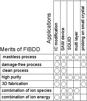
Relationship between merits and applications
ü@
Surface acoustic wave device
ü@
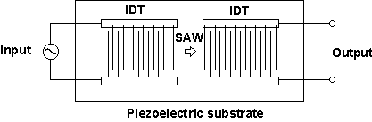
Principle of surface acoustic wave (SAW) devices
ü@
Expected features of direct deposited interdigital transducers (IDT)
1.High power capability
2.Flexible design
ü@
Experiment
Fabrication of bandpass filter
Substrate : LiNbO3 (64üŗYX)
IDT : direct deposited Au,Cu,Al
ü@
Pictures of SAW sample
ü@
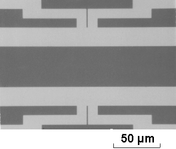
Before deposition of IDT
ü@
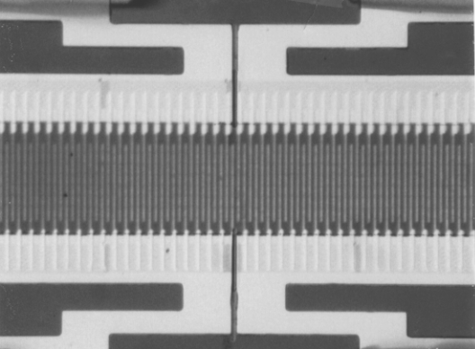
After deposition of IDT
ü@
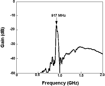
Measured characteristics of fabricated sample
(direct deposited Al IDT 41pairs/41pairs, 4.8 ā╩m period)
ü@
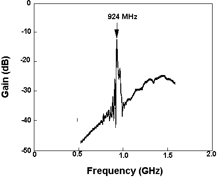
Measured characteristics of referenced sample
(Al IDT 81pairs/81 pairs, 4.8 ā╩m period)
ü@
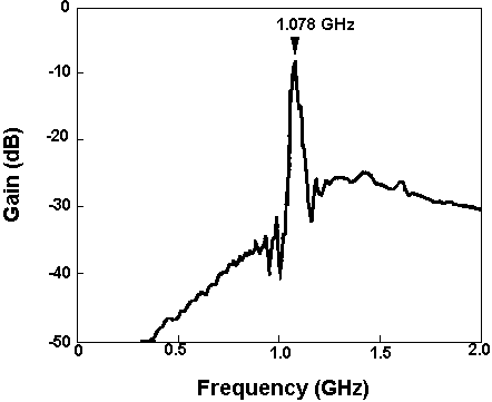
Measured characteristics of fabricated sample
(direct deposited Au IDT 41pairs/41pairs, 4 ā╩m period)
ü@
Lower insertion loss was observed.
ü@
ü@
Superconducting quantum interference device(SQUID)
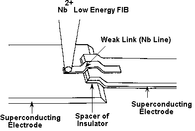
Weak link fabrication of Quasi-Planar-Josephson-Junction
ü@
Expected feature of direct deposited weak link :
Controllability and reproducibility of critical current
ü@
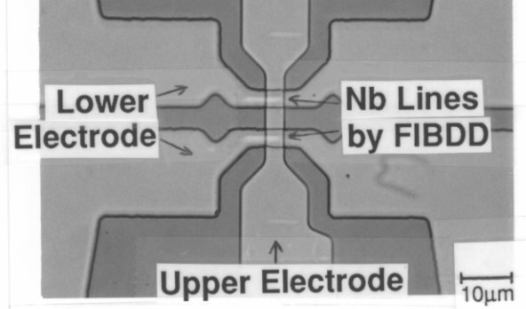
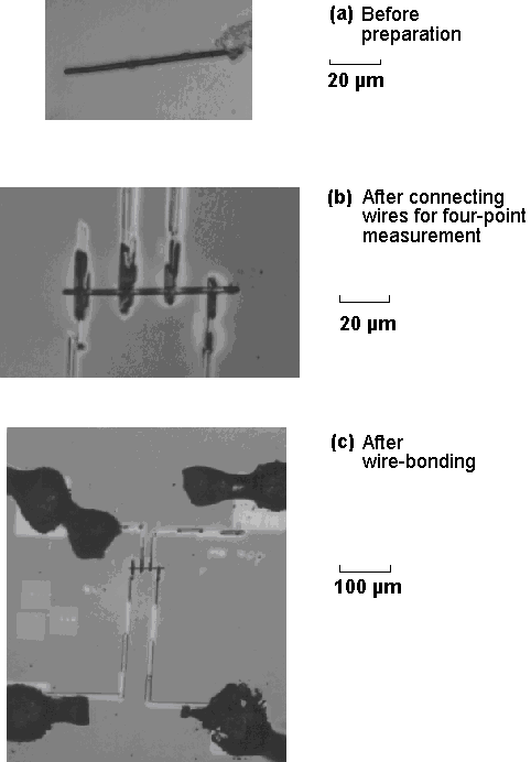
Photograph of Josephson Junctions
ü@
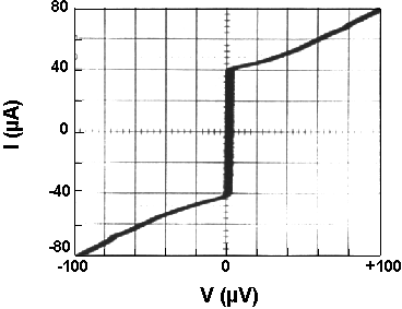
I-V curve of fabricated Josephson Junction
ü@
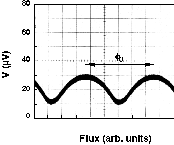
H-V curve of fabricated DC-SQUID
ü@
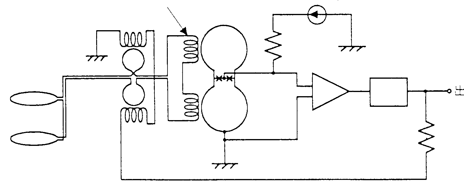
Diagram of DC-SQUID circuit
ü@
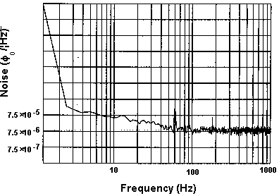
Noise characteristics of fabricated DC-SQUID
ü@
Performance of DC-SQUID was comparable to ordinary tunnel junction DC-SQUID.
ü@
ü@
Co/Cu multilayer
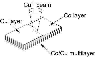
Fabrication of Co/Cu multilayer
with 108 eV Co2+ beam and 54 eV Cu+ beam
(Cu-Co-Nb-Au alloy ion source)
ü@
Expected features :
1.Magnetic/nonmagnetic multilayer
2.Controllability of thickness
3.Giant magnetoresistance (GMR) effect
Experiment:
1.Fabricate Co/Cu multilayer
108 eV Co2+ beam and 54 eV Cu+ beam
14X76 ā╩m2
2.0 nm Co 12 layers and 1.3 - 2.2 nm Cu 11 layers
2.Form probe electrodes
54 eV Au+ beam
ü@
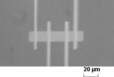
Photograph of fabricated sample
ü@
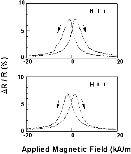
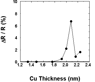
Measured MR ratio (dR/R) as a function of applied magnetic fields
ü@
ü@
Measured MR ratio (dR/R) as a function of Cu layer thickness
ü@
GMR effect was observed.
Precise controllability of thickness
ü@
Probing on small crystal
ü@
ü@
Restrictions on applications
ü@
1.Sample size
Deposition time by 10 nA beam
100 ā╩m x 100 ā╩m x 0.1 ā╩m : 17 minutes
10 mm x 10 mm x 0.1 ā╩m : 116 days
2.Mass production
Processing time for 1 sample
FIBDD : ~1/2 day
Photo-lithographic process : 1 week ~ 1 month
ü@
Processing time for 1,000,000 samples
FIBDD : > machine life
Photo-lithographic process : 1 week ~ 1 month
ü@
Conclusions
ü@
We developed some applications of FIBDD and proved that FIBDD is a useful tool for research and development.
ü@