Focused ion beam direct deposition
and its applications
Å@
2.Low energy FIB apparatus
for direct deposition
Å@
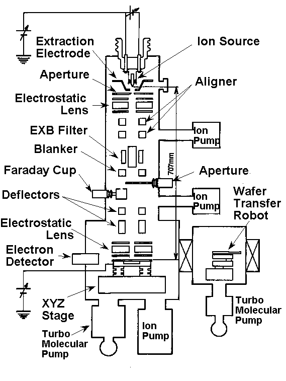
Demanded capabilities:
Å@
Low energy (<100 eV) and
Small beam diameter (<1µm)
Large beam current density
Å@
Alloy ion source and mass filter
Patterning by deflector and sample stage
Sample observation by optical microscope
Low residual gas pressure
Quick sample exchange
Å@
Diagram of FIB apparatus for direct deposition
Å@
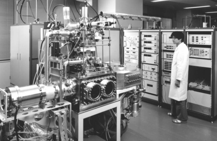
Picture of FIB apparatus for direct deposition
Å@
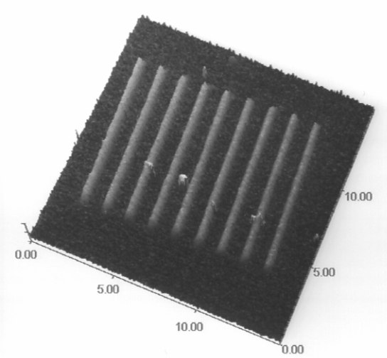
AFM image of a direct deposited Au lines
( 32 eV Au+ on Si substrate)
Å@
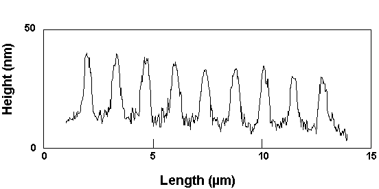
A cross section profile
Å@
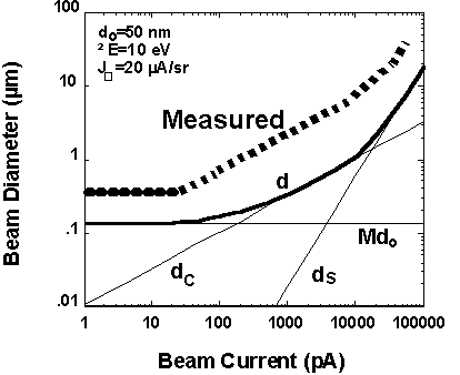
Calculated beam diameter and
measured 50 eV Au+ beam diameter
Å@
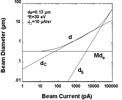
Recalculated beam diameter for Au+ beam
Å@
How to get finer beam or
higher beam current density :
Å@
Improvements of ion source
Reduced source size
Reduced energy dispersion
Increased angular current density
Å@
Improvements of optics
Reduced Magnification
Reduced chromatic aberration
Å@
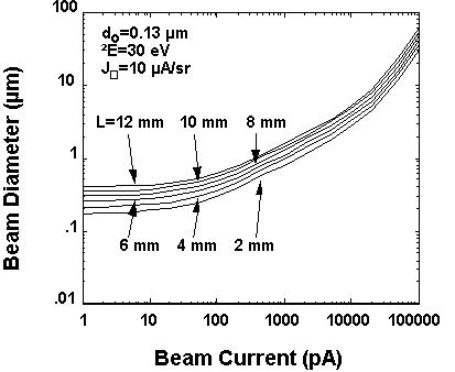
Example of improvement
(calculated for 50 eV Au+ beam, L=deceleration length)
Å@
Development of Ion Source
Impregnated-electrode-type LMIS
Å@
For conductive material (Au,Cu,Al)
Au-Si alloy LMIS
Au-Cu alloy LMIS
Au-Cu-Si alloy LMIS
Au-Cu-Ge alloy LMIS
Al-Au-Ge alloy LMIS
Au-Cu-Al alloy LMIS
Au-Cu-Al-Ge alloy LMIS
Å@
For superconductive material (Nb)
Nb-Au-Cu alloy LMIS
Å@
For magnetic material (Co)
Cu-Co-Nb-Au alloy LMIS