MOD 4: RF AMP Modification
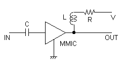
Put RF MMIC AMP on RF stage. The circuit diagram is shown fig 2.
RF gain will gain of 15-20dB, NF will better about 2dB by this MOD.
*** This MOD is very risky. Please ask your skill before trying. The better way to improve RF gain and NF is putting a high gain and low NF priamplifier between an antenna and a converter. ***
| MMIC | Gain
[dB] | NF
[dB} | V
[V] | R
[ohm] | C
[pF] | L |
| ERA-3 | 20 | 4.5 | 5.0 | 51
(>1/16W) | 100
or
1000 | optional
(10nH-
10uH ??) |
| ERA-5 | 19 | 4.0 | 5.0 | 0 |
* ERA-3 and ERA-5 are from Mini-Circuits
* Gain and NF are the specification of the MMIC
fig 2: RF AMP circuit
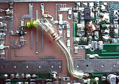
Photo 9: RF AMP
Modification
- (1) Parts
- Shown in Fig 2 is the RF AMP circuit diagram and parts list. A bias resistor R is depended on the MMIC.
- (2) PC board MOD
- Remove a capacitor pointed by blue arrow on photo 10.
- Tear a part of the pattern showing red arrow on photo 10. The RF AMP circuit is located here.
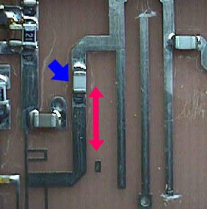
Photo 10: Remove capacitor showed by blue arrow and tear pattern
- (3) RF AMP
- Return a capacitor removed at (1) on the same place.
- Put a DC blocking capacitor C on another end of the pattern.
- Put a MMIC between the capacitors and soler it. Be sure the MMIC direction. Ground pin is solered to the left capacitor. The point is just Ground. An another side of MMIC ground pin remains open.
- Extra leads should be cut before soldering.
- Power supply point showing photo 12 is out side of RF and IF shield case. A bias resistor R should be covered with tube to insulate the shield case. Form the resistor lead going through the shield case hole and solder it to the power supply point. Solder the another side of the resistor lead to MMIC output pin. A choke L may be put between the resistor and MMIC output pin.
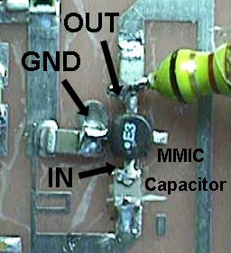
photo 11: RF AMP
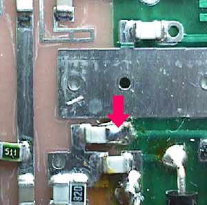
photo 12: Power supply point
Back to Converter Main Page /
Previous Page